|
Implementation
of
Digital
Modulation
on SpinCore PulseBlasterDDS And
RadioProcessor Boards
Introduction:
Digital modulation
is used to
transfer a digital bit stream over an analog channel at a high
frequency.
This enables us to transmit signals generated in a digital circuit
across a physical medium. This is because digital signals can be
handled with higher security and digital systems are readily and widely
available.
Depending on which parameter of the carrier signal is varied in
accordance with the digital message signal, we obtain three main
variants of digital modulation called Amplitude
Shift Keying (ASK), Frequency
Shift Keying (FSK) and Phase
Shift Keying (PSK).
Amplitude Shift Keying
(ASK)
In ASK the
amplitude of the transmitted
carrier signal is varied in accordance with the logic levels of the
message signal.
SpinCore PulseBasterDDS Board Implementation For ASK:
On the SpinCore PulseBasterDDS board, the Amplitude Shift
Keying waveform is generated using NCO, by controlling the gating
and/or
amplitude registers with respect to the input logic sequence using the
PulseBlaster Timing Core.
The demo source code written here gives the flexibility of choosing
the different bit rate and the length of the input sequence and
specifying the amplitude
of the carrier for different logic bits.
Note that the bit rate can not be faster than (clock/9) for proper
results.
The
complete
C
code demonstrating this implementation will be provided with the next
version of SpinAPI, but for now can be found here. It uses a
sinusoidal waveform as the carrier signal. The carrier is
generated using a similar technique to that used for analog modulation.
Note that this code can be extended to the more general case of an
M-ary baseband signal as well (such as quantizing a two or three bits
at a time instead of one bit).
Inputs to the program are:
- Carrier signal frequency
- Amplitude for a logic 1
- Amplitude for a logic 0
- Length of the message signal
- Logic sequence comprising the message signal.
Output: ASK modulated waveform.
If the amplitude level for the carrier wave transmitted is either "0"
or "1"
for logical values of "0" and "1" respectively then we can
use the pb_inst_radio
instead of pb_inst_radio_shape.
This
is
because
pb_inst_radio does not allow us to select amplitude
registers.
The following SpinAPI function is used to load the Amplitude registers:
pb_set_amp(amp0,
0);
pb_set_amp(amp1,
1);
The total number of amplitude levels in the carrier waveform depends on
the
total number of the amplitude registers available on the board being
used. If you would like a board with more amplitude registers, please
contact SpinCore.
The program allows the user to choose any amplitude values between 0.0
and
1.0 for the two logic levels. Amplitude register values are
programmed with respect to the input
logic values and sequence. The sample code is as shown below for the
same. They are controlled and fed accordingly by
the PulseBlaster Timing
Core.
for
(i=0;i<length;i++)
{
if(!seq[i])
{
pb_inst_radio_shape(0,0,0,0,
TX_ENABLE,
NO_PHASE_RESET, NO_TRIGGER,
NO_SHAPE, 0, 0x00,CONTINUE, 0, tm*us);
}
else
{
pb_inst_radio_shape(0,0,0,0,
TX_ENABLE,
NO_PHASE_RESET, NO_TRIGGER,
NO_SHAPE, 1, 0x0F,CONTINUE, 0, tm*us);
}
}
The parameter passed after the "NO_SHAPE" parameter
in the above code specifies the correct amplitude register for the ith
bit in the logic sequence, as specified by the user.
ASK waveforms generated using the example code are shown in the figures
below.
|
Figure
1
shows
an ASK waveform generated using the code.
Channel
1
shows
the output ASK for a carrier frequency of Fc = 0.5
MHz and a baseband signal bit rate of 100 kbps. The amplitude for a
logic 0 = 0.0 V and the amplitude for a logic 1 = 1V. The message
signal was chosen to be the logic
sequence "10101".
Channel
2
shows
the input modulating signal. i.e. input message (logic
sequence) signal with bit rate = 100 kbps.
|
|
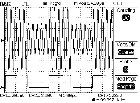
Figure 2 shows
another
ASK waveform generated using the example code.
Channel
1
shows
the output ASK for a carrier frequency of Fc = 0.5
MHz and a baseband signal bit rate of 100 kbps. The amplitude for a
logic 0 = 0.5 V and the amplitude for a logic 1 = 1V. The message
signal was chosen to be a logic
sequence "10101".
Channel
2
shows
the input modulating signal. i.e. input message (logic
sequence) signal with bit rate = 100 kbps.
|
|

Figure
3
shows
output
ASK waveform generated using the example code.
Channel
1 shows the output ASK for a carrier frequency of Fc = 0.5
MHz and a baseband signal bit rate of 100 kbps. The amplitude for
a logic 0 = 0.5 V and the amplitude for a logic 1 = 1V. The message
signal was chosen to be a logic
sequence "10011001".
Channel
2 shows the input modulating signal. i.e. input message (logic
sequence) signal with bit rate = 100 kbps.
|
Frequency Shift Keying
(FSK)
In FSK the
frequency of the transmitted
carrier signal
is varied in accordance with the logic of levels of the message signal
while keeping the
amplitude constant.
SpinCore PulseBasterDDS Board Implementation For FSK:
On the SpinCore PulseBasterDDS board, the Frequency Shift
Keying waveform is generated using the NCO, by controlling the
frequency
registers with respect to the input logic sequence using the
PulseBlaster Timing Core.
The demo source code written here gives the flexibility of choosing a
different bit rate and the length of the input sequence and
specifying the phase
of the carrier for different logic bits.
Note that the bit rate can not be faster than (clock/9) for proper
results.
The
complete
C
code demonstrating this implementation will be provided with the next
version of SpinAPI, but for now can be found here. It
uses a sinusoidal waveform as a carrier signal. The carrier is
generated using a similar technique to that used for analog modulation.
Note that this code can be extended to the more general case of an
M-ary baseband signal as well.
Inputs are:
- Frequency to transfer for logic 1
- Frequency to transfer for logic 0
- Length of the message signal.
- Logic sequence comprising the message signal.
Output: FSK modulated waveform.
Following SpinAPI function is used to load the Frequency registers:
pb_set_freq
(fc1*MHz);
pb_set_freq(fc2*MHz);
Total number of unique frequency changes in the carrier waveform with
respect to logic levels depends on the total number of the Frequency
registers available.
The program allows the user to choose any frequency values between 1
and 100 MHz. for the two logic levels.
Frequency register values are programmed with respect to the input
logic values and sequence.
They are controlled and fed accordingly by the PulseBlaster Timing
Core.
The sample code is as shown below for the same.
for
(i=0;i<length;i++)
{
if(!seq[i])
{
pb_inst_radio(0,0,0,0,
TX_ENABLE,
NO_PHASE_RESET, NO_TRIGGER,
0x00,CONTINUE, 0, tm*us);
}
else
{
pb_inst_radio(1,0,0,0,
TX_ENABLE,
NO_PHASE_RESET, NO_TRIGGER,
0x0F,CONTINUE, 0, tm*us);
}
}
The first parameter passed in the pb_inst_radio instruction above
corresponds to the chosen frequency for the ith bit in the logic
sequence defined by the user.
Outputs for the different frequencies of the carrier signal
for different logic pulses are shown
below.
|

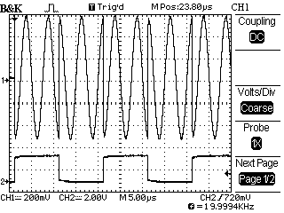
Figure 4 shows an
FSK waveform generated using the source code on a PulseBlasterDDS board.
Channel
1
shows
the output FSK for a carrier frequency for logic level 0 is
Fc(0) = 0.5
MHz and for logic level 1 is Fc(1) = 1 MHz.
Channel
2
shows
the input modulating signal. i.e. input message (logic
sequence) signal with bit rate = 100 kbps and logic
sequence = "10101".
|
|

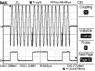
Figure 5 shows the
FSK waveform generated using the example source code but this time with
some different parameters.
Channel
1
shows
the output FSK for carrier frequency for logic level 0 is
Fc(0) = 0.2
MHz and for logic level 1 is Fc(1) = 2 MHz.
Channel
2
shows
the input modulating signal. i.e. input message (logic
sequence) signal with bit rate = 100 kbps and logic
sequence = "10101".
|
|
Figure
6
shows
output
FSK waveform generated using the example source code but with different
length sequence of input message signal
Channel
1
shows
the output FSK for carrier frequency with logic level 0
is Fc(0) = 0.2
MHz and for logic level 1 is Fc(1) = 1 MHz.
Channel
2
shows
the input modulating signal. i.e. input message (logic
sequence) signal with bit rate = 100 kbps and logic
sequence = "10011001".
|
Phase Shift Keying
(PSK)
In PSK, the
phase of the transmitted
carrier signal
is varied in accordance to the logic of levels of the message signal
while keeping the
amplitude constant.
SpinCore PulseBasterDDS Board Implementation For PSK:
The PSK implementation shown here is implemented on the PulseBlasterDDS
and RadioProcessor boards using similar methods to FSK.
The Phase Shift
Keying waveform is generated using the NCO, by controlling the phase
registers with respect to the input logic sequence using the
PulseBlaster Timing Core.
The demo source code written here gives the flexibility of choosing
the different bit rate and the length of the input sequence and
specifying the phase
of the carrier for different logic bits.
Note that the bit rate can not be faster than (clock/9) for proper
results.
The
complete
C
code demonstrating this implementation will be provided with the next
version of SpinAPI, but for now can be found here.
It
uses a sinusoidal waveform as a carrier signal. The carrier is
generated using a similar technique to that used for analog modulation.
Note that this code can be extended to the more general case of an
M-ary baseband signal as well.
Inputs are:
- Phase corresponding to a logic 1
- Phase corresponding to a logic 0
- The frequency of the carrier signal.
- Length of the message signal.
- Logic sequence comprising the message signal.
Output: PSK modulated waveform.
Following SpinAPI function is used to load the Phase registers:
pb_set_phase
(phase1);
pb_set_phase(phase2);
The total number of unique phase changes in the carrier waveform with
respect to logic levels depends on the total number of the phase
registers available. If you would like to have more phase registers
available, please contact SpinCore.
The program allows the user to choose any phase values between 0
and 360 degrees for the two logic levels.
Phase register values are programmed with respect to the input
logic values and sequence.
They are controlled and fed accordingly by the PulseBlaster Timing
Core.
The sample code is as shown below for the same.
for
(i=0;i<length;i++)
{
if(!seq[i])
{
pb_inst_radio(0,0,0,0,
TX_ENABLE,
NO_PHASE_RESET, NO_TRIGGER,
0x00,CONTINUE, 0, tm*us);
}
else
{
pb_inst_radio(0,0,0,1,
TX_ENABLE,
NO_PHASE_RESET, NO_TRIGGER,
0x0F,CONTINUE, 0, tm*us);
}
}
The fourth parameter above shows the outputting of the corresponding
phase to the ith bit in the logic sequence, as defined by the user.
Outputs for the different values of phase of the carrier signal
for different logic pulses are shown
below.
|
Figure
7
shows
the PSK waveform generated using the example source code on a
PulseBlasterDDS board.
Channel
1
shows
the output PSK of a carrier signal with phase for logic 0 as
phase(0) = 0 degrees and
for logic 1 as phase(1) = 180 degrees and having a carrier frequency =
200 kHz.
Channel
2
shows
the input modulating signal. i.e. input message (logic
sequence) signal with bit rate = 100 kbps and logic
sequence = "10101".
|
|
Figure
8
shows
the PSK waveform generated using the example source code but
with different
input parameters.
Channel
1
shows
the output PSK of a carrier signal with phase for logic 0 as phase(0) = 90 degrees and for
logic 1 as phase(1) = 270 degrees and having a carrier frequency = 200
kHz.
Channel
2
shows
the input modulating signal. i.e. input message (logic
sequence) signal with bit rate = 100 kbps and logic
sequence = "10101".
|
|
Figure
9
shows
output
PSK waveform generated using the example source code for different
length of input message signal.
Channel
1
shows
the output PSK of a carrier signal with phase for logic
level 0 as phase(0)
= 0 degrees and for logic level 1 as phase(1) = 270 degrees and having
a carrier
frequency = 200 kHz.
Channel
2 shows the input modulating signal. i.e. input message (logic
sequence) signal with bit rate = 100 kbps and logic
sequence = "10011001".
|
These are only the basics of what you can do using SpinCore's
PulseBlasterDDS and RadioProcessor boards. Please see the manuals
of the boards and source code examples in SpinAPI for more details.
|


 Contact Us | Software Downloads